Cesky: |
How Sharp GDG was dissected
Every "my precious" eight-bit deserves a replica. Which sometimes requires special parts. Spectrists can still get their ULA, but what about poor "my precious" Sharp MZ800 and its GDG (Graphic Display Generator)? And so I became suspicious when the thread "Sharp MZ - GDG photo chip" appeared on the OldComp forum on 11/20/2018. suksoft writes: "So a small miracle happened. Mikes21 successfully managed to take a photo of our GDG chip in the MZ800. It cost him a day of his life, a long working trip and some money, but the result is of high quality."
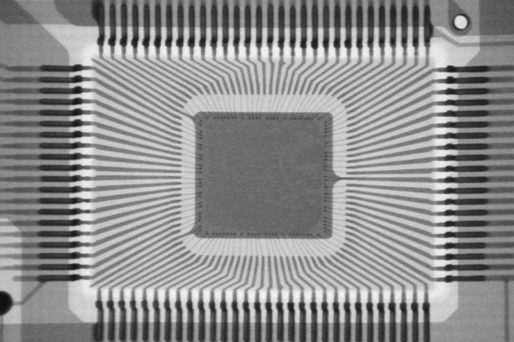
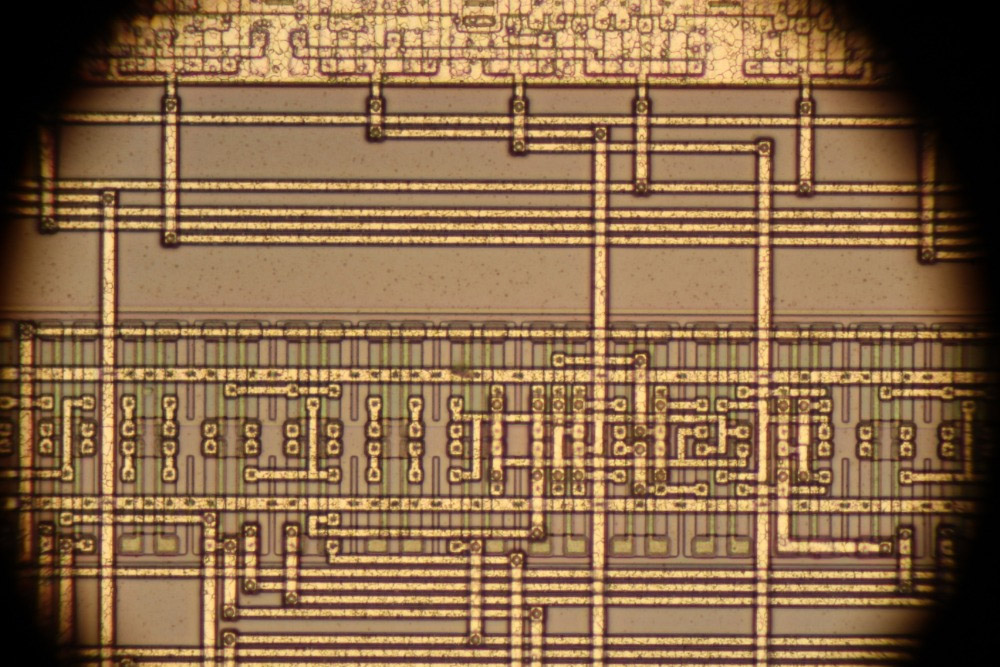
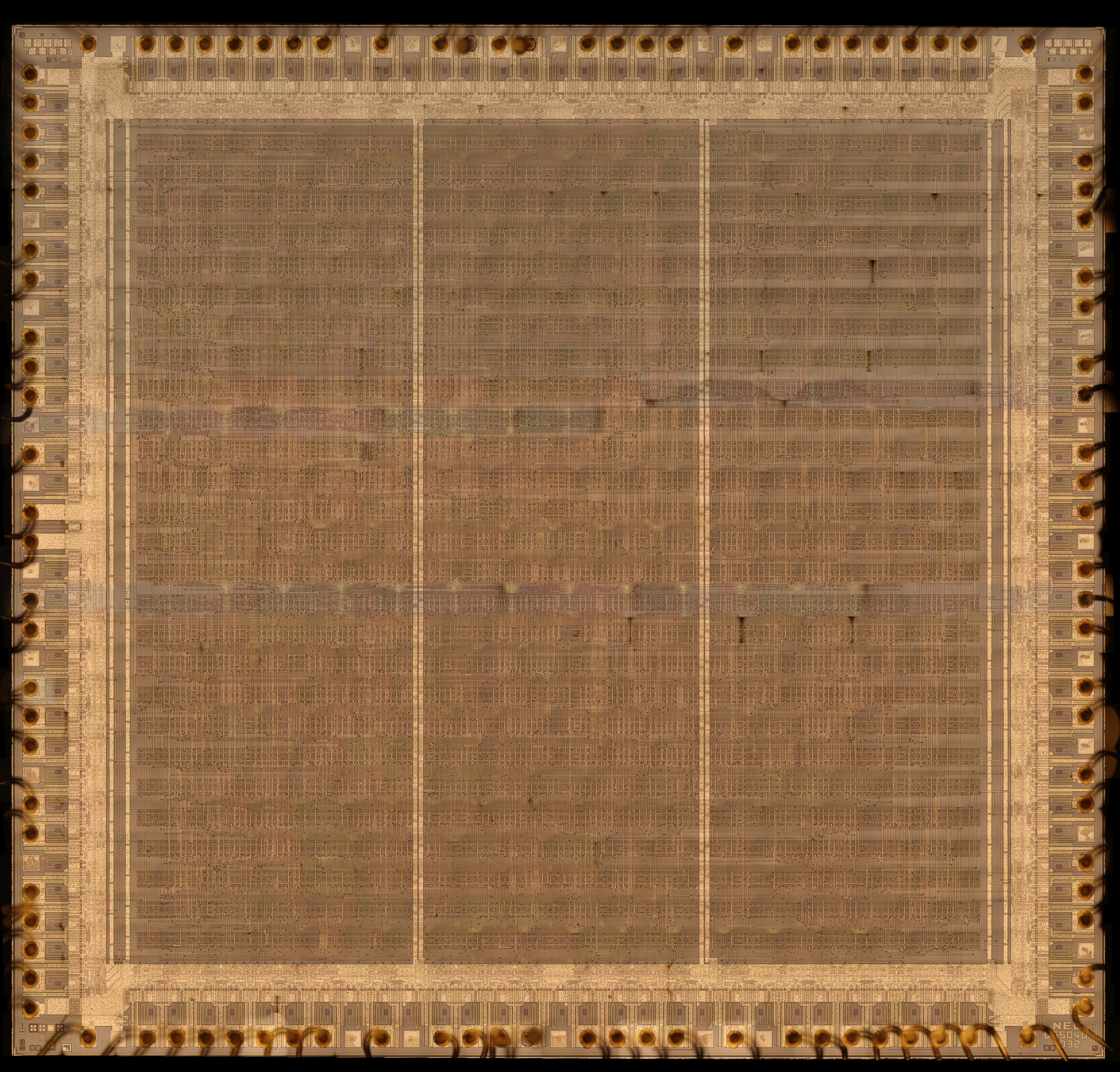
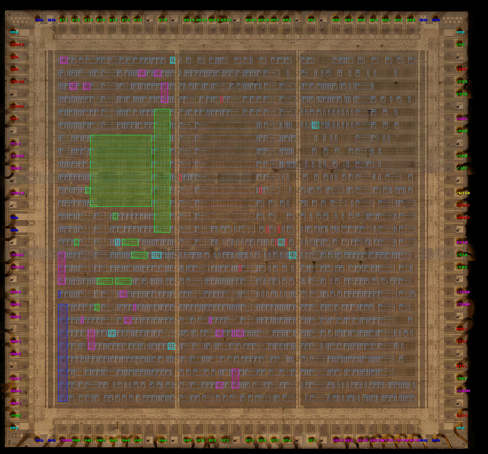
The GDG chip was manufactured by the NEC, under the designation uPD65040 (datasheet), a 100-pin 2-micron CMOS gate array with 4104 cells organized in 27 x 152 matrix. Of course, one cannot expect to read the contents from a single overall image; nothing would be discernible from the details.
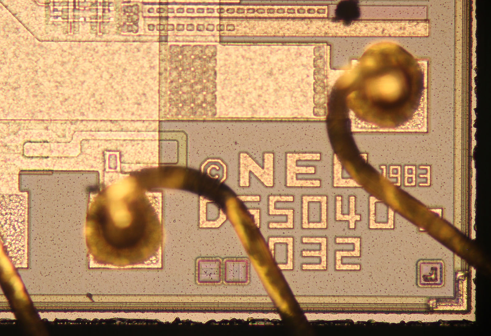
The designation in the bottom right corner of the chip is NEC 1983 D65040 032.
115 images were taken at 20x magnification (12 rows of 9 or 10 images) and 734 images at 50x magnification (31 rows of 22 to 26 images). The size of one image is 5184 x 3456. The original plan was to get a few enthusiasts together to split the images and decipher the content.
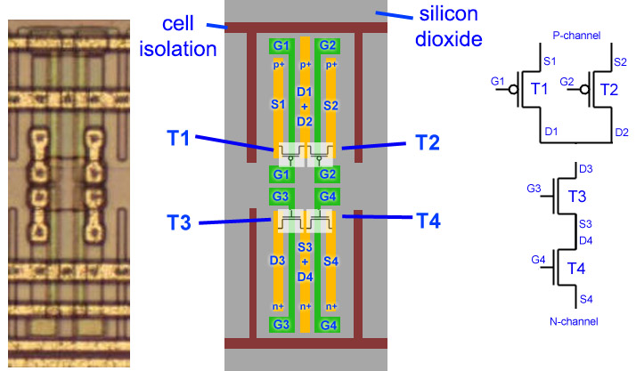
The base cell consists of 4 transistors: two P-channels and two N-channels, with double-layer metal interconnects. The first layer usually makes horizontal connections, the second layer vertical. The upper thick horizontal connection feeds the VCC supply, the lower thick horizontal connection is GND ground.
Several gates were deciphered in earlier experiments two years ago, but only 32 cells were photographed. Now it's finally become realistic to decrypt the entire chip. I also started to dabble a bit (like Panda38) and tried to decode a few cells as well.
Unused cell:
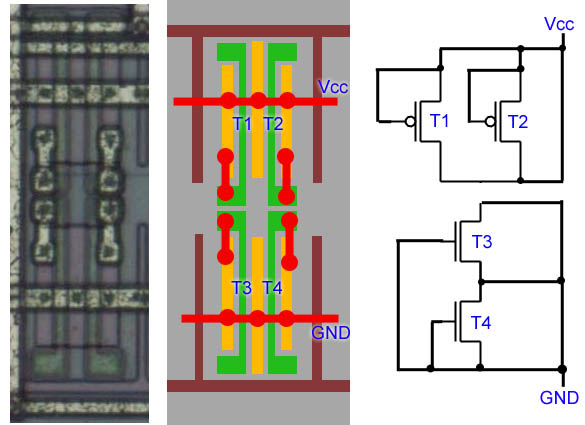
Invertor:
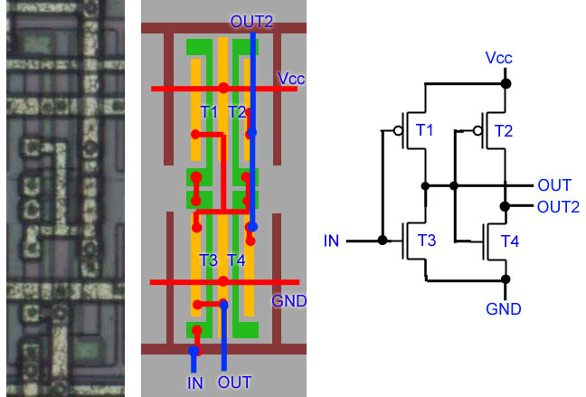
2-input NAND gate:
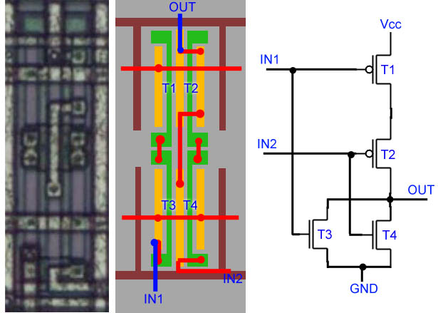
2-input NOR gate:
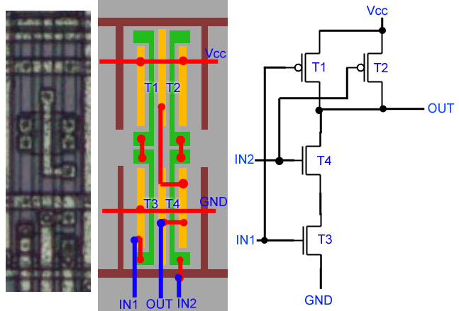
3-input NAND gate:
It turned out to be a necessary step to first assemble all the images into one large array, in which each cell would have its exact coordinate, so that the tasks could be automated. The images from the microscope did not have the exact position, they had overlaps, a little skewed and darkened edges ... of course, there was no better way to realise this. Normalization into a single image would have helped a lot in subsequent procedures.
I created a program to generate an image of the assembly. It goes through the input images row by row and column by column. First it performs a brightness correction - normalizes the overall brightness of the image and lightens the edges. It creates differential images. Instead of luminance information, the differential image contains luminance changes between neighboring pixels. The differential images are used to find overlap between the images. They are preferable to luminance images because they are less dependent on luminance differences. To find the overlap, the correlation of the images is calculated - the sum of the squares of the pixel differences of the images is calculated. The images are shifted relative to each other and the minimum correlation is found - this corresponds to the most similar image overlap. This is how the images in each row are aligned to each other. By finding the correlation of the first image in the row, the rows are correctly matched together. A skew correction is performed on the images, which corrects for the rotation of the images. This aligns the cell images to the exact coordinate grid. Alternatively, the program can still draw the coordinate grid into the resulting image. Example of a differential image:
During the generation I unfortunately found that rows 12 and 17 are not contiguous, there are 2 missing scans of 2 rows. They are replaced from 20x magnification - it's a lower quality image, deciphering is more difficult, but even with that it was eventually successful. Below is a download of the generator program, along with the source images and the generated assembly in 1/4 reduction, with and without raster. When run, the program will generate the assembly file (it's 21 GB, image size 90544 x 84268 pixels), the individual segments and the scaled images of the assembly. The generation takes one hour. The resulting full resolution image cannot be displayed in any graphical editor due to its excessive size, it must be processed programmatically.
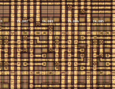
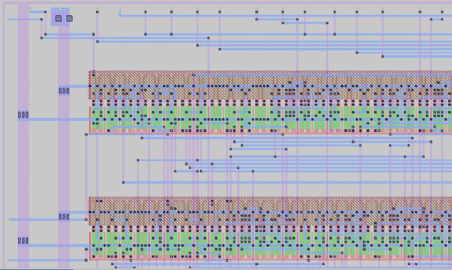
Cells with grid. There are 4 vertical grid lines per cell, 106.125 pixels apart, and 16 horizontal grid lines, 74.215 pixels apart. Between cells there are 18 horizontal grid lines with a spacing of 68.357 pixels. The cell number indicates the row and column of the cell.
In order to decrypt the cells, it was necessary to cut the image into individual cells. For this purpose I prepared the program GDG_cell (download below). The gdg.bin report file is placed in the folder, the program generates the images with the cells and prepares the gdg_cell.csv list, which would contain the cell types.
Now it is time to decode the function of each cell. While it would be possible to recognize the wire jumper and function of each cell manually, it can be very difficult due to the signals attached, where each cell looks different. I tried to use a neural network to help me with the detection. I have used the neural network to decode images before, I had a C++ library created for this purpose with Cuda support.
The program to detect cell types is also available for download below. During the detection process, I have been drawing samples of the gate types. They are labeled according to the NEC datasheet. The samples can also be found in the archive provided.

There is a neural network detection program in the gdgnet folder. The program uses an image of the assembly in 1/4 size gdg4.jpg. As an auxiliary image it uses gdg16gray.tga, a scaled down grayscale image. When the program runs, the neural network first learns from the samples it finds in the type folders. After learning, it tries to detect previously unknown images. It generates and stores the images in the type folders. This is followed by a manual correction phase. It goes through the type folders and checks whether the type has been correctly determined. If not, the definition can be corrected by moving it to the correct folder or deleting it, leaving the detection to automation. After correction, a new automatic detection is performed. This is done in a row-by-row fashion. In the configuration file, parameters are set - for which rows the network should learn and which rows to detect. Once the cells in the initial rows are correctly detected, the network becomes increasingly successful in detecting them, and subsequent rows become easier to analyze. The result is a gdg_gate.csv file containing the definition and coordinates of each gate. This takes into account that some gates occupy several cells.
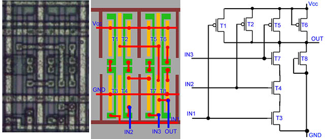
Later I helped with analysis of pins and input/output gates - see archive below. But I didn't actively participate in the analysis of the GDG chip anymore, so I will continue only very briefly. The main ant work rested on suksoft, Mikes21, microlan, uunek. suksoft prepared the editor for defining the connections, microlan made the connections, Mikes21 analyzed the circuit function with the Magic simulator and defined the circuit diagram. They tested the function, redrawn, refined, debugged, corrected errors.
Analysis of hazard states:
Complete replacement "schematic" of the chip:
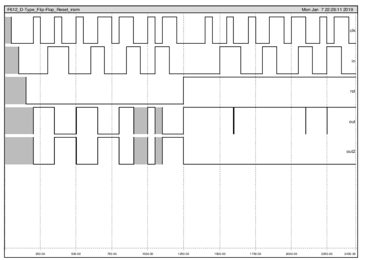
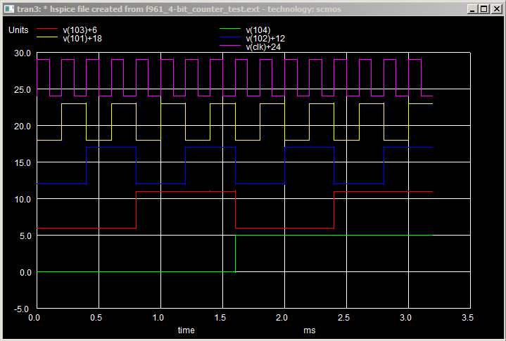
The F961 counter is finally reading, the wipers are wiping:
After 4 months of work, the first celebrations:
Mikes21
wrote: BINGO! I have the same thing. It's a split of 5, so IHMO
it looks absolutely great.
This is a complete milestone. The base path is paved and looks
functional. This is a date to remember.

Redrawing the schematic into Eagle:
Mikes21 wrote: I would like to make a small milestone or recapitulation of today. Panda, after previous analysis of the gates, identified and documented all types of surrounding pins and assigned to each its function. Chaky wrote converters for digital simulation, especially for VHDL. He wrote definitions of all gates so they can be used in the simulator and also various test functions. He is now debugging a data unification routine for Radek. They are looking for and trying to remove various differences and ambiguities. At the moment Microlan is in the 'backup' searching and clarifying every discrepancy. He remembers the whole cipher by heart and, without looking at the computer, reports exactly where it is and what needs to be corrected. Vasek is working his way through the GDG simulation and sometimes I have to hold my breath when I see his progress. Please hang in there, the sharpists are watching you. Quite a few people are watching this whole thing more or less closely, and I think many of them don't even bother to look. Every once in a while, there's a shot, and maybe some people don't even know which one is hitting. Am I right? Guys, a huge thank you and praise to all of you in front of the sharpist community, currently scattered across several republics of this world. Before embarked military unit, it will be (that compliment) for sure on the nearest Tal mill (not yet on the horizon). You have made an indelible mark on the history of the world. (And yet it is such a ...)
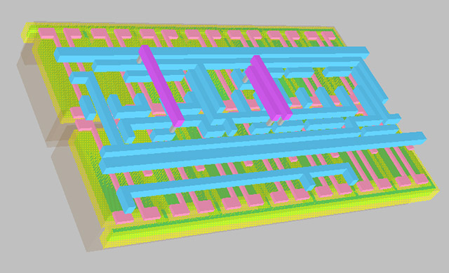
Adder in 3D:
Current status after 3/4 year of work:
Mikes21
wrote: Just to add:
- there is an entire (almost, like 99%) documented chip from the
silicon perspective
- there is a complete analysis of the circuitry at the transistor
level
- we have a complete analysis and simulation of all gates used,
including I/O pins.
- There is a conversion to gate level, such as flip-flop circuits
and counters
- there is a 3D model for visualization (or for 3d printing?)
- we have export to basic model description in VHDL and
SystemVerilog
- we can simulate a chip on the analog level, it is very time
consuming
- we simulate at the SPICE model level.
- We are learning to use TechBench on the level of VHDL and
SystemVerilog
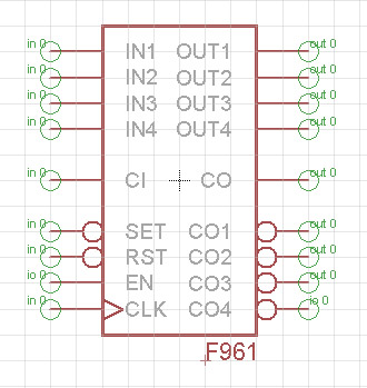
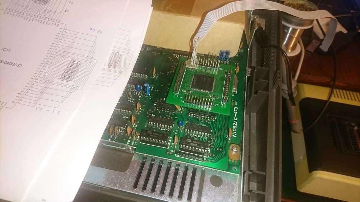
Exactly after a year, the work reached the state when the adapter for connecting the CPLD (Altera 5M1270ZT144C5) to the real Sharp was prepared and the implementation of the code in VHDL was being prepared. The following is the merging of the circuits into functional units and the analysis of the function of the GDG parts. suksoft is testing the counters for PAL signal generation in the FPGA:
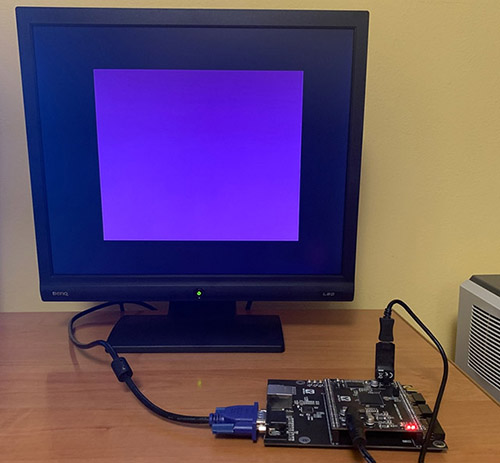
May 2020, after a year and a half, Mikes21 revives and programs its CPLD adapter. The first hints of functionality of the emulated GDG.
And after another month of debugging and finding bugs (incorrect micro line readings and delays), finally success with image generation.
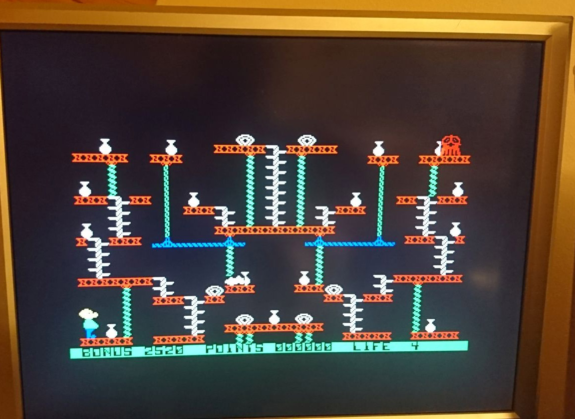
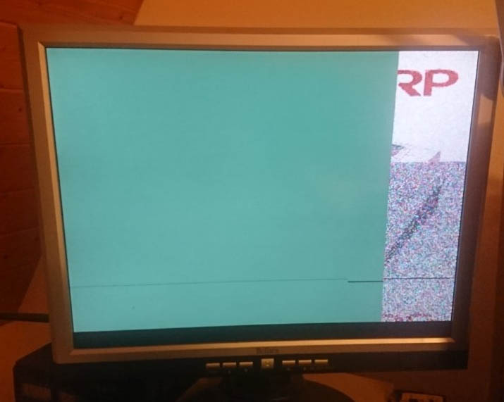
Martin8bity tries the GDG emulation in Altera MAX V CPLD and confirms that the image is perfectly identical to the original GDG. GDG implemented with CPLD seems to be fully functional, except for some minor tweaks. suksoft continues to decrypt GDG functions.
The "GDG_draw" program to colour mark the functional parts of the GDG chip:
Downloads
Assembly generator (4 parts of 550 MB each): part 1, part 2, part 3, part 4
Cutting the gdg.bin assembly into individual cells (474 KB): GDG_cell
Gate type analyzer with neural network (280 MB): GDG_net
Pins and input/output gates (28 MB): GDG_pins
Image of GDG chip with pins in 1/4 size, size 22014 x 21067 pixels (103 MB): piny4.jpg
Program to colour mark the functional parts of the GDG chip (140 MB): GDG_draw
Miroslav Nemecek